Huawei Technologies has announced a groundbreaking chip design framework, "LogicFolding," and a new "Tau Scaling Law." This initiative is a direct response to U.S. sanctions, aiming to circumvent restrictions on advanced semiconductor technology and manufacturing equipment. The company claims this new approach prioritizes signal speed and data throughput over traditional transistor miniaturization, potentially offering a path to high-performance chips without relying on Western-made EUV lithography machines.
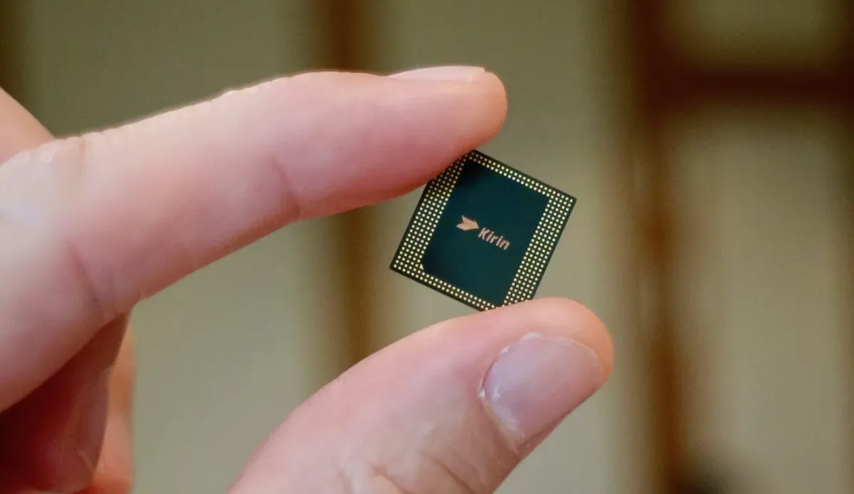
The LogicFolding architecture, refined over six years, involves physically folding and stacking logic circuits. Huawei plans to debut this technology in its upcoming Kirin smartphone processor for the Mate 90 handset this autumn, with aspirations to apply it to AI processors and data centers by 2030. This strategic move signifies China's ongoing commitment to achieving semiconductor self-sufficiency and could significantly alter the global competitive landscape.