Huawei Technologies Co. Ltd. has introduced a novel chip design framework, dubbed "LogicFolding," alongside a new "Tau Scaling Law," aiming to bypass stringent U.S. sanctions and advance China's semiconductor capabilities. This development, announced at the IEEE International Symposium on Circuits and Systems in Shanghai, represents a strategic pivot away from traditional semiconductor scaling methodologies, particularly Moore's Law, which has become increasingly difficult to pursue due to export restrictions on advanced manufacturing equipment. Huawei's initiative signifies a concerted effort to bolster domestic chip production and reduce reliance on foreign technology, potentially reshaping the global semiconductor landscape.
The announcement comes at a critical juncture, as the U.S. continues to tighten its grip on China's access to cutting-edge semiconductors and the sophisticated EUV lithography machinery required for their production. Huawei's proposed Tau Scaling Law diverges from Moore's Law by prioritizing signal speed and data throughput optimization over the physical miniaturization of transistors. This new paradigm, implemented through the LogicFolding architecture, involves physically folding and stacking logic circuits within a dual-layer framework. The company claims this approach significantly reduces internal wiring lengths, thereby minimizing signal delays and leading to substantial improvements in transistor density and power efficiency. This innovation could provide Huawei with a means to develop high-performance chips without requiring access to the most advanced Western manufacturing technologies.
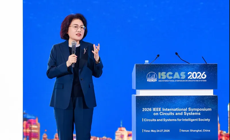
Huawei's Innovative Chip Architecture and Scaling Law
The LogicFolding architecture, developed over six years of intensive research and development, is Huawei's proprietary solution to the challenges posed by international sanctions. According to He Tingbo, a board member and chairman of Huawei's HiSilicon Semiconductor division, the company has successfully designed and validated 381 chips using this new blueprint. This architectural innovation is designed to optimize the flow of data across a system, focusing on how rapidly information can be processed rather than solely on transistor size. By reconfiguring the physical layout of circuits, Huawei aims to achieve performance parity with, or even surpass, chips manufactured using conventional methods, all while operating under severe technological restrictions.
The underlying Tau Scaling Law, as explained by Huawei, represents a "temporal scaling framework." Instead of focusing on the geometric shrinking of transistors, it emphasizes enhancing the speed and efficiency of data transfer. This temporal optimization is crucial for future advancements in computing, particularly in areas like artificial intelligence and high-performance computing, where data processing speed is paramount. Huawei's approach suggests a potential new direction for chip design, one that may prove more resilient to geopolitical pressures and supply chain disruptions that have impacted the global technology sector.
Commercial Debut and Future Applications
Huawei plans to introduce its new Kirin smartphone processor, built on the LogicFolding architecture, with the upcoming launch of its flagship Mate 90 handset this autumn. This marks the commercial debut of the technology and its adherence to the new Tau Scaling Law. The company has ambitious plans to extend this architecture to its Ascend AI processors, which serve as alternatives to Nvidia's graphics processing units (GPUs), and integrate it into high-capacity artificial intelligence data centers by 2030.
Looking further ahead, Huawei projects that by 2031, it will be capable of producing chips that match the performance of Western-made 1.4-nanometer (nm) processors. This timeline places Huawei in direct competition with industry leaders like TSMC, which aims to mass-produce 1.4nm chips by 2028. This aggressive roadmap underscores Huawei's commitment to regaining technological autonomy and its potential to disrupt the established semiconductor hierarchy, even amidst ongoing trade restrictions.
Strategic Implications and Industry Impact
The unveiling of Huawei's new chip architecture and scaling law is a significant development, reflecting China's broader strategy to achieve self-sufficiency in critical technologies. This move comes with substantial investment from the Chinese government in domestic chipmaking capabilities and the pursuit of alternative technological pathways. The announcement has already had an impact on the stock market, with shares of Semiconductor Manufacturing International Co. (SMIC), China's largest contract chip manufacturer, surging by over 19%. This indicates a positive market reception and reinforces the perception of a potential breakthrough that could significantly mitigate the impact of U.S. sanctions.
Industry analysts acknowledge the potential significance of Huawei's innovation. While the ultimate success of the LogicFolding architecture and Tau Scaling Law remains to be seen, it represents a viable alternative path forward for China's semiconductor industry in the face of unprecedented supply chain challenges. If Huawei can execute its ambitious timeline, this development could not only enhance its own competitive standing but also signal a broader shift in global semiconductor manufacturing and geopolitical dynamics. The company's ability to develop and scale these advanced technologies independently will be a key indicator of its resilience and future trajectory.
Impact Analysis
Huawei's announcement of the LogicFolding architecture and Tau Scaling Law has profound implications for the global semiconductor industry. It demonstrates a potential circumvention of U.S. sanctions, allowing China to advance its domestic chip production capabilities without relying on Western technology or manufacturing processes. This could lead to a bifurcation of the global semiconductor market, with China developing its own ecosystem independent of traditional supply chains. The emphasis on temporal scaling rather than purely geometric shrinking also represents a fundamental challenge to the long-standing paradigm of Moore's Law, potentially ushering in a new era of chip design focused on performance optimization through architectural innovation rather than just miniaturization.
For Western semiconductor companies and governments, this development poses a significant strategic challenge. It underscores the need for continuous innovation and adaptation in the face of evolving geopolitical landscapes and technological competition. The success of Huawei's initiative could reduce its dependence on foreign technology, impacting market share for global leaders and prompting a re-evaluation of export control strategies. Furthermore, it highlights the growing importance of national industrial policies in driving technological advancement and semiconductor sovereignty, a trend that could accelerate the global race for technological dominance.